Nanofabrication Central Facility Instrumentation
Lithography
Heidelberg MLA 150 Maskless Aligner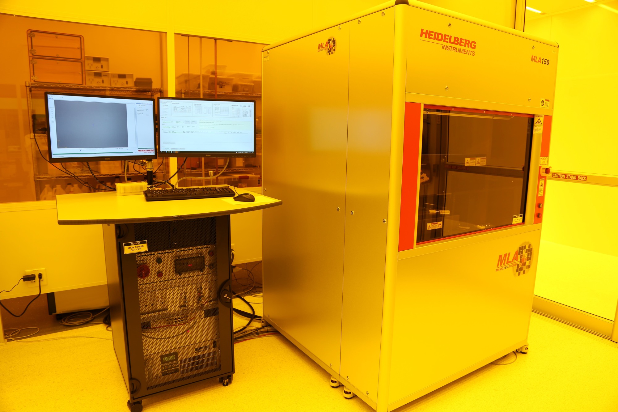
The Heidelberg MLA 150 Maskless Aligner is a high-speed, direct-write, optical lithography system to fabricate nano- and micro-patterned materials and surfaces at low-cost and over large areas. The instrument has two laser illumination modules, optical systems to steer the laser beams and control exposure, integrated cameras for high-accuracy alignment to pre-existing structures, automated translation stage, real-time pneumatic autofocus, and a class 10 climate controlled chamber to achieve photo-lithographically defined structures with feature size ≤1μm.
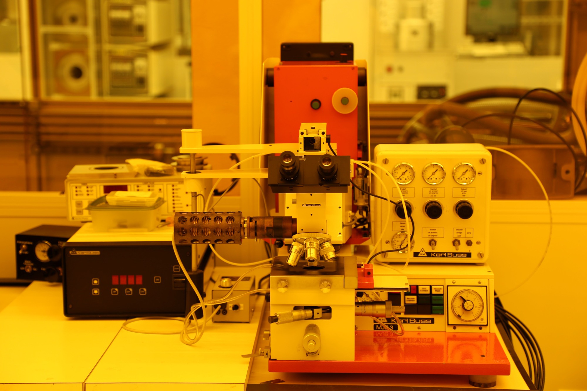
Karl Suss MJB3 UV300 Mask Aligner
The Karl Suss MJB3 UV300 3-inch Mask Aligner is designed for high-resolution photolithography, with a 350 W mercury lamp and Suss diffraction-reducing exposure optics. The primary exposure wavelengths of 365 or 403 nm lead to roughly 1 µm minimum feature size. For smaller feature sizes, electron-beam lithography is available in the Electron Microscope Facility.
Newport-Oriel Flexible Mylar-Mask Lithography System
Newport-Oriel Flexible Mylar-Mask Lithography System is designed for printing from flexible Mylar masks onto substrates as large as 4” x 4” square or 5” diameter. It is capable of printing 5-micron features with placement and alignment to approximately 2 microns with appropriate alignment marks.
Nano Imprinter
The Nano Imprinter system offers thermal and UV nanoimprint and imprinting in vacuum if needed. The system transfers the patterns, usually nanohole or nanopillar arrays, from a silicon stamp to a nanoimprint-polymer-coated substrate by applying heat and pressure.
Thin Film Deposition
Angstrom Engineering Electron-Beam Thin Film Deposition System
The Angstrom Engineering Electron-Beam Thin Film Deposition System is a state-of-the-art tool for high-precision thin-film fabrication, supporting both single-layer and automated multi-layer deposition of metals, dielectrics, and oxides. Thin-film deposition is a critical step in micro- and nano-fabrication, often representing the final (“back-end”) process required to produce fully functional microelectronic, nanoelectronic, and photonic devices.
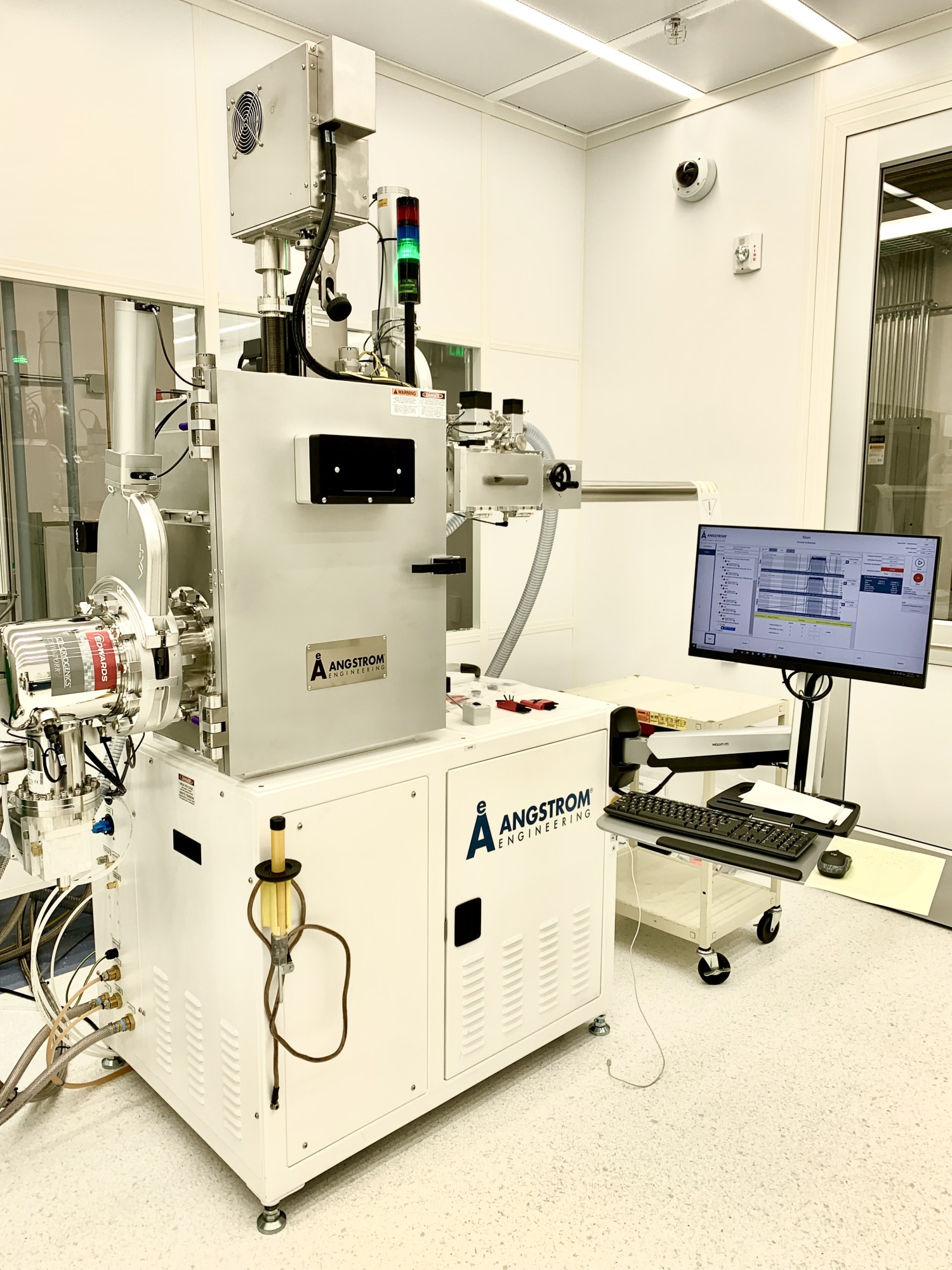
This system combines high-rate e-beam evaporation with fully automated multi-layer deposition, allowing sequential deposition of multiple materials or complex stacks without breaking vacuum. The result is ultra-clean interfaces, excellent reproducibility, and robust device performance.
Key Features & Capabilities:
- High-rate deposition of metals, dielectrics, and oxides
- Capability for refractory metals with high melting points
- Line-of-sight deposition ideal for high-yield lift-off processes
- Automated multi-layer deposition for complex metal and dielectric stacks
- Ultra-low base pressures for contamination-free, high-purity films
- Supports applications in microelectronics, MEMS, photonics, and sensors
Currently Available Deposition Materials:
- Aluminum (Al)
- Chromium (Cr)
- Copper (Cu)
- Germanium (Ge)
- Gold (Au)
- Platinum (Pt)
- Silicon Dioxide (SiO₂) (dielectric/oxide)
- Titanium (Ti)
Available Automated Recipes
- Ti/Au sequential deposition
- Cr/Au sequential deposition
Additional single-layer and multi-layer recipes, including metal/dielectric stacks, can be developed upon request to support custom research needs.
This advanced system significantly enhances NCF’s thin-film deposition capabilities, providing researchers with a reliable, high-performance platform for creating well-defined metal contacts, multilayer devices, and complex thin-film stacks for next-generation microelectronics, MEMS, sensors, and photonics.
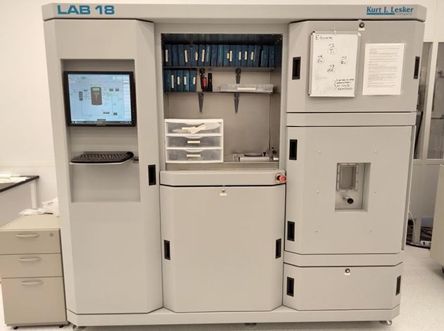 Lesker Lab-18
The Lesker Lab-18 thin film deposition system is a combined electron-beam evaporator and RF sputtering Physical Vapor Deposition (PVD) system that makes high quality, research-grade metallic, semiconducting, and dielectric thin films. The Lab 18 includes a four-pocket electron beam evaporator as well as two 2” magnetron sputter sources. Two mass flow controllers regulate the chamber pressure and gas composition for reactive sputtering.
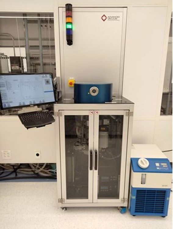
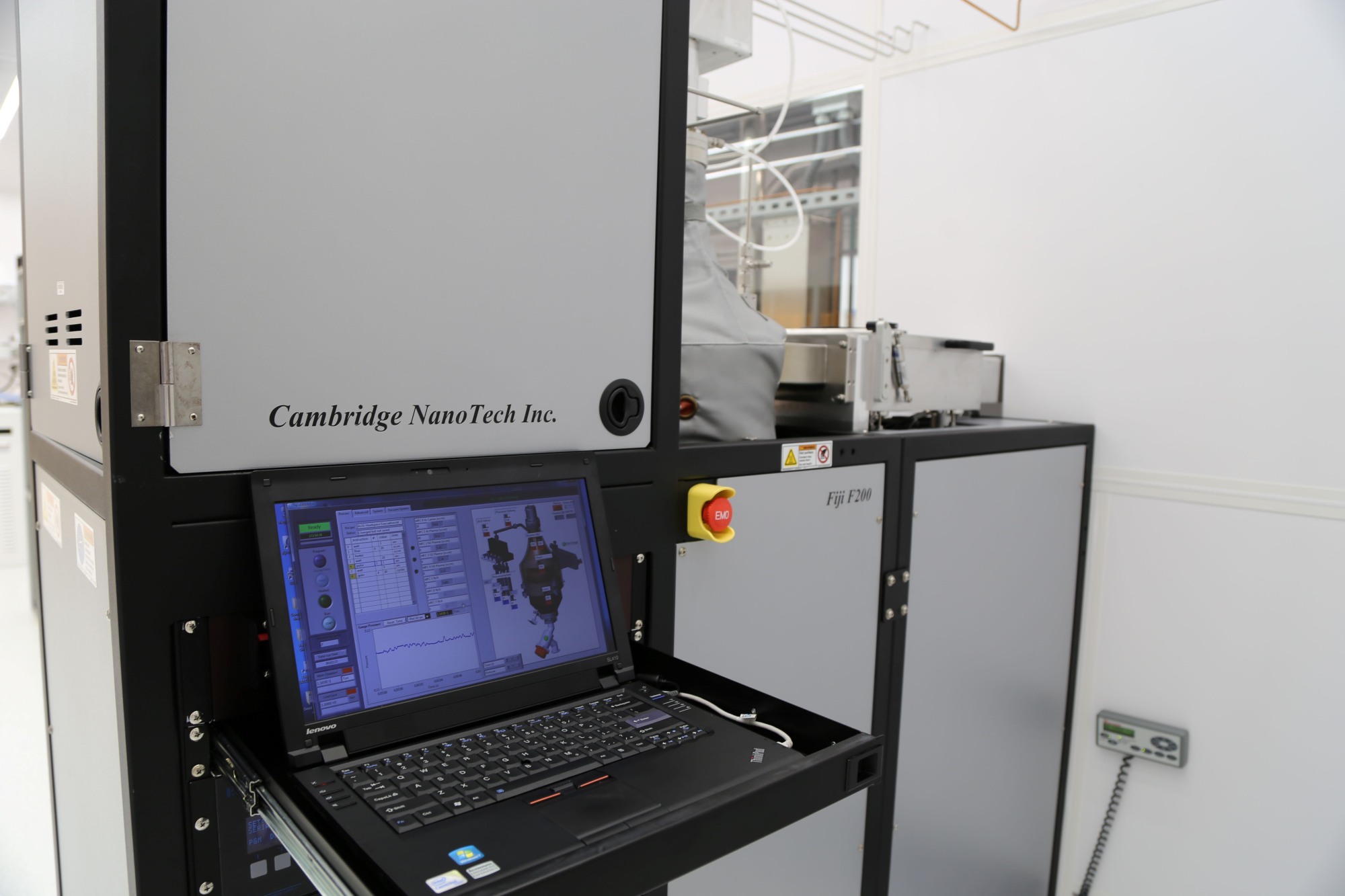 Cambridge NanoTech Fiji F200 Atomic Layer Deposition System
The Cambridge NanoTech Fiji F200 series Atomic Layer Deposition (ALD) System is a modular medium to high-vacuum system that accommodates a wide range of deposition modes. This tool is currently configured with precursors for metallic and oxide layers of Hafnium, Aluminum and Tungsten.
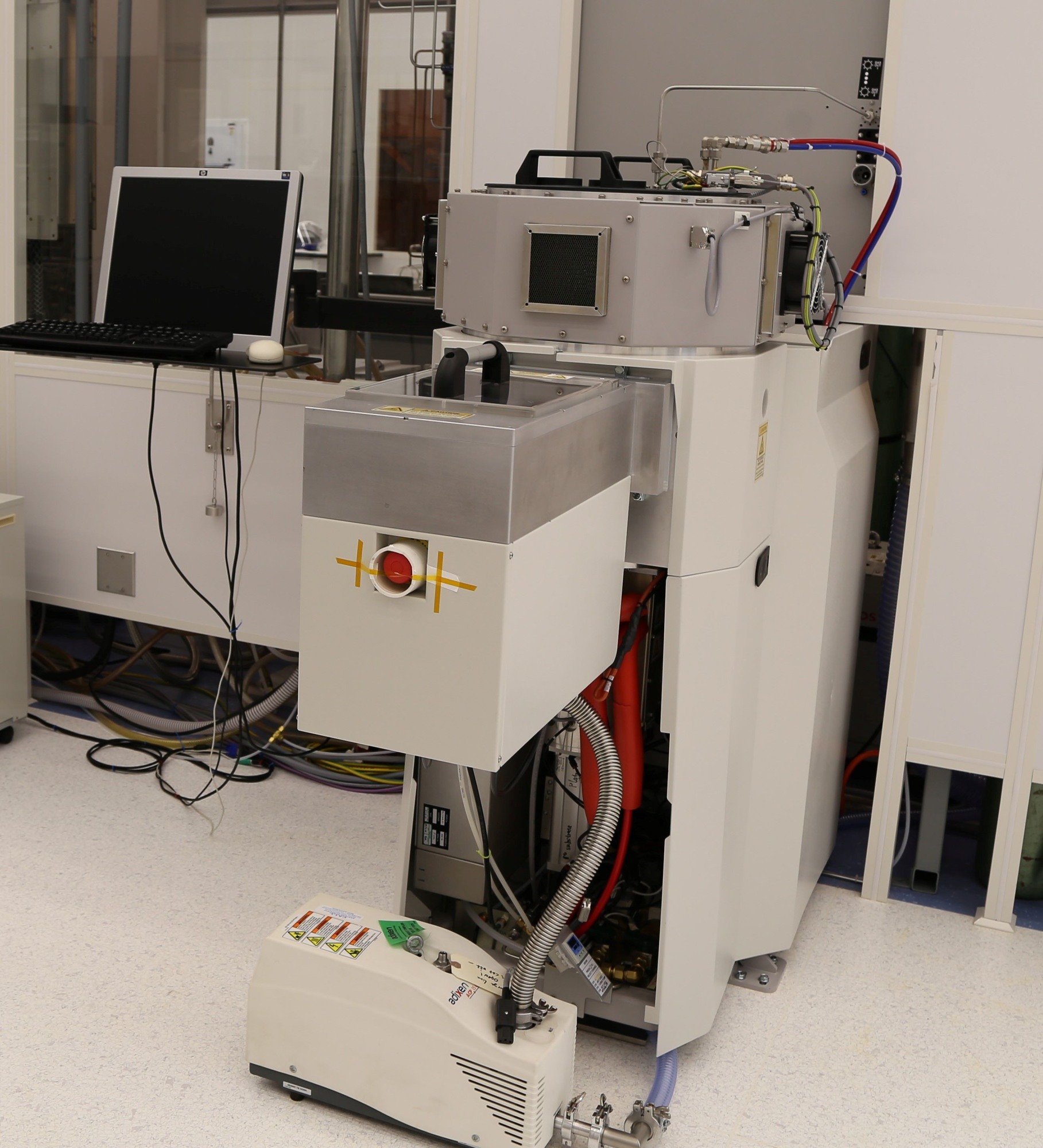
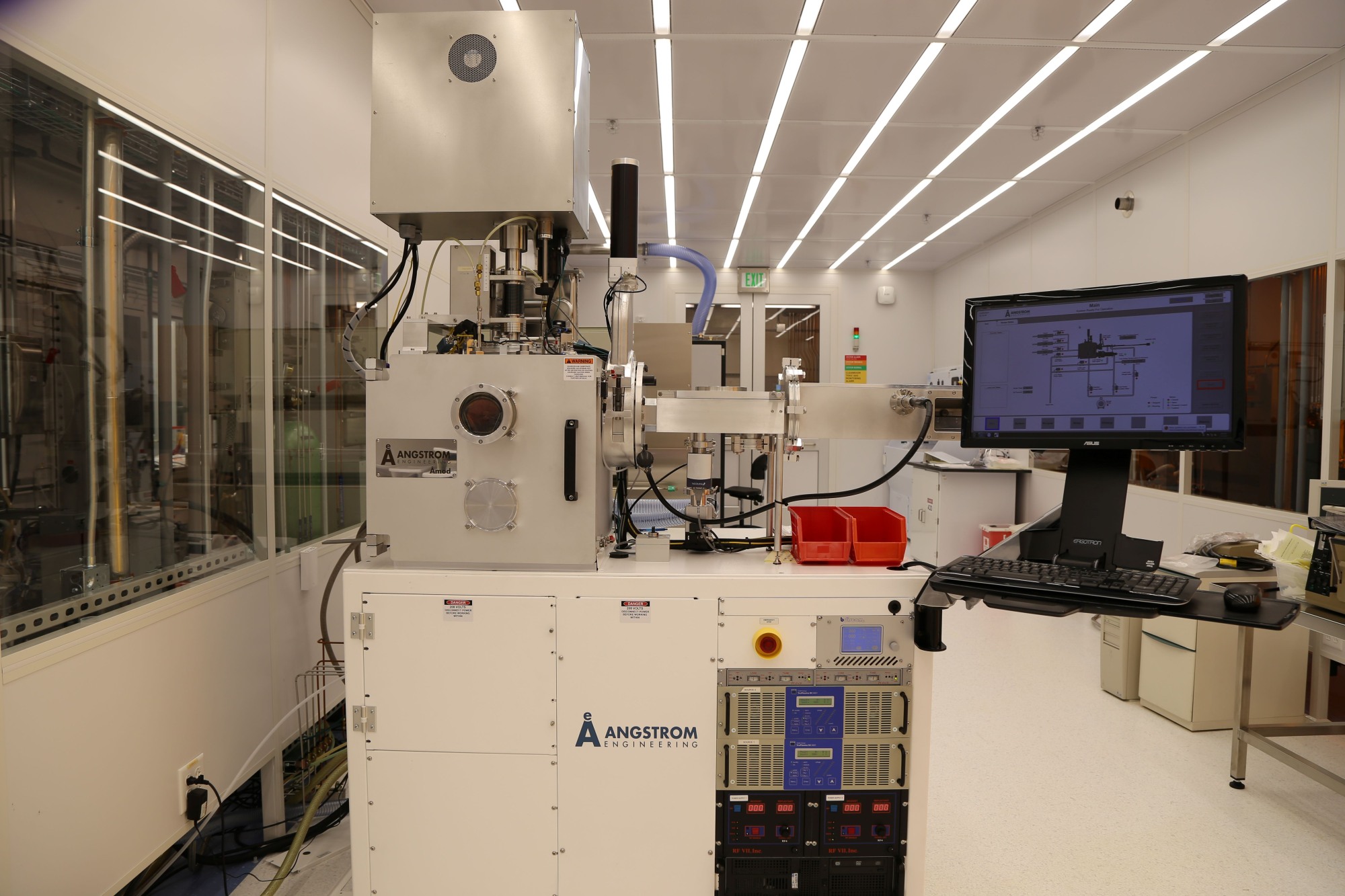 Angstrom Multi-Target Sputtering System
The Angstrom Multi-Target Sputtering System accommodates four 3-inch sputtering sources and a variety of PVD processes (RF and DC). The temperature of the substrate can be increased up to 800˚C.
Physical Etching
AJA International Orion Series Argon Ion Mill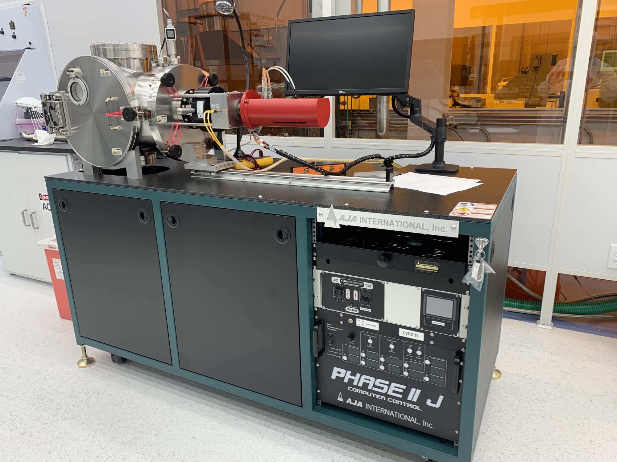
Ion mills etch samples by direct physical sputtering of material using a large diameter, neutral beam of Argon ions incident on the substrate surface at an angle to prevent redeposition of the sputtered material. Since the etching process is physical rather than chemical, it is applicable to a wide range of sample materials. Argon milling produces smooth surfaces the shape of which may be defined photolithographically. The Orion mill has a water cooled, rotating (0 – 20 RPM) substrate holder that accepts up to 4” diameter substrates. The ion energy is adjustable from 100 eV to 1200 eV at currents up to 120 mA. The incident angle of the beam to the substrate surface can be varied over -/+ 90° to optimize the etch rate and sidewall definition.
Plasma Etching
 PlasmaTherm Vision 320 RIE System
The Vision 320 RIE provides etch capability for R&D, prototyping, and low volume production. This parallel-plate capacitance based systems is found in applications that include fundamental material studies, surface modification, semiconductor device fabrication. The Vision 320 is a manual load, reactive ion etcher (RIE) configured for fluorine based etching. Etch gases connected to the system are CF4, CHF3, SF6 and O2. Common materials etched in fluorine chemistries include silicon oxide (SiO2), silicon nitride (Si3N4), and isotropic etching of silicon and fluorine etchable metals. The platen is a 10” graphite plate capable of holding sample pieces up to a 10” substrate.
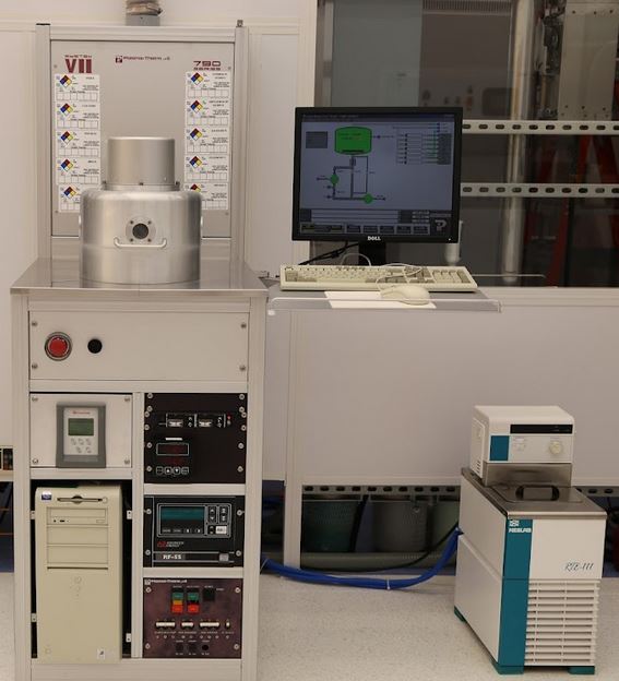 PlasmaTherm 790 RIE-PECVD System (Fluorine-chemistry)
The PlasmaTherm Model 790 RIE-PECVD system has a computer-controlled single-wafer turbopumped chamber that provides reactive ion etching (RIE) and plasma-enhanced chemical vapor deposition (PECVD) capabilities. RIE is accomplished using fluorine-chemistry gases (CF4, CBrF3, CHF3, SF6, etc.) with up to 500 W RF power. PECVD capability provides low-temperature (up to 300 °C) SiO2 and Si3N4 deposition from silane chemistry.
 SPTS LPX Inductively Coupled Plasma RIE System
The SPTS LPX is an inductively coupled plasma (ICP) reactive-ion etcher (RIE) that offers the ability to etch very-deep, high-aspect-ratio structures, especially silicon, silicon dioxide, and silicon nitride. This system is configured with a range of gases for reactive- and physical-ion etching (i.e. SF6, C4F8, CF4, O2, and Ar). The LPX-ICP system is equipped with a single-wafer load-lock transfer arm for 100mm wafers; smaller wafers and small pieces may be processed on the system using a carrier wafer.
Characterization
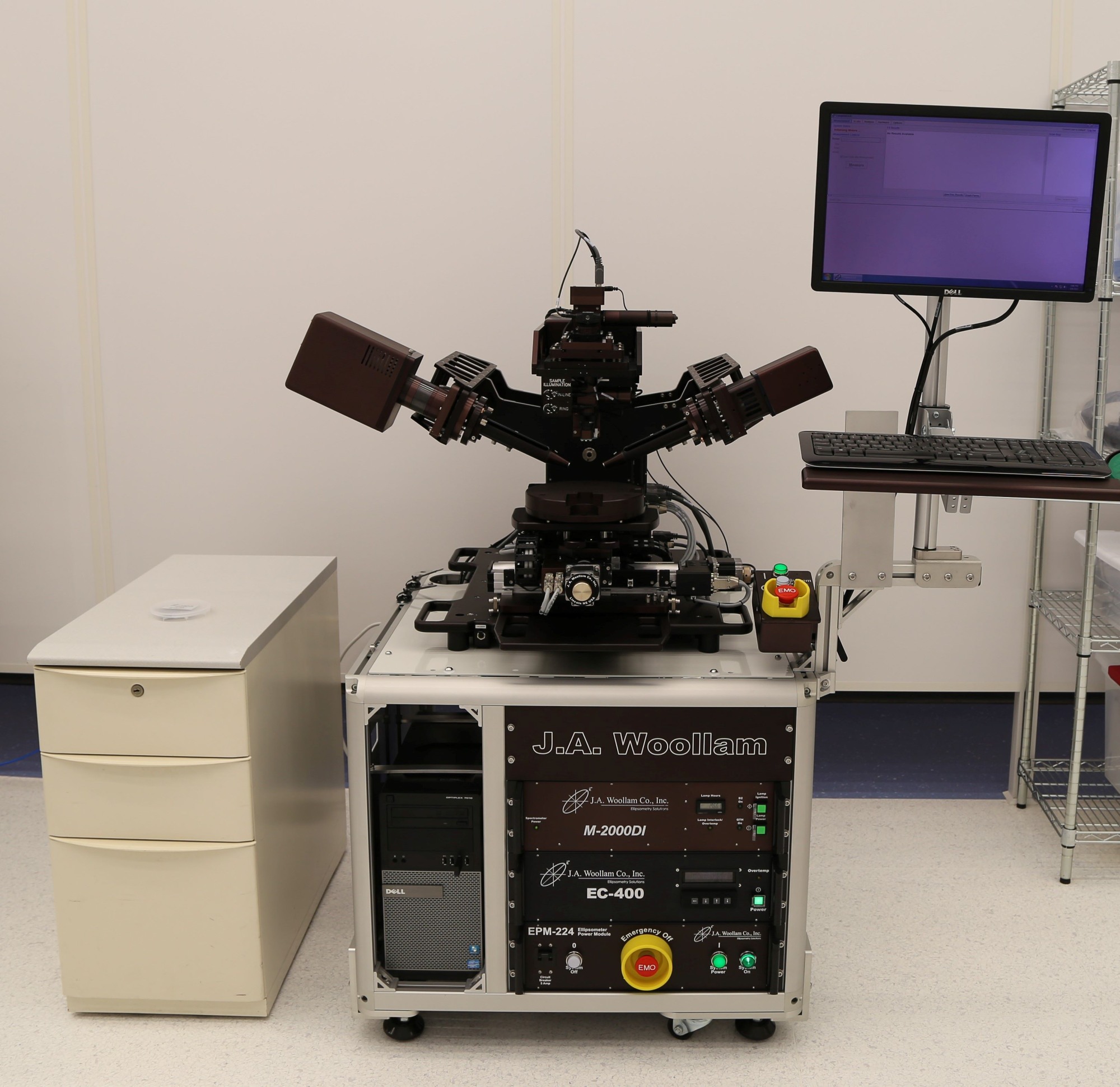
JA Woollam M-2000 Ellipsometer
The JA Woollam, M-2000 Variable Angle Research Grade ellipsometer measures angle- and wavelength-dependent reflectivity and transmissivity data over a wide spectral range (from ultraviolet to near-infrared) that is analyzed to directly to determine optical properties of single- and multi-layer films (e.g., their thickness and complex wavelength-dependent refractive index), which provide insight into their underlying chemical, electronic, and mechanical properties.
DektakXT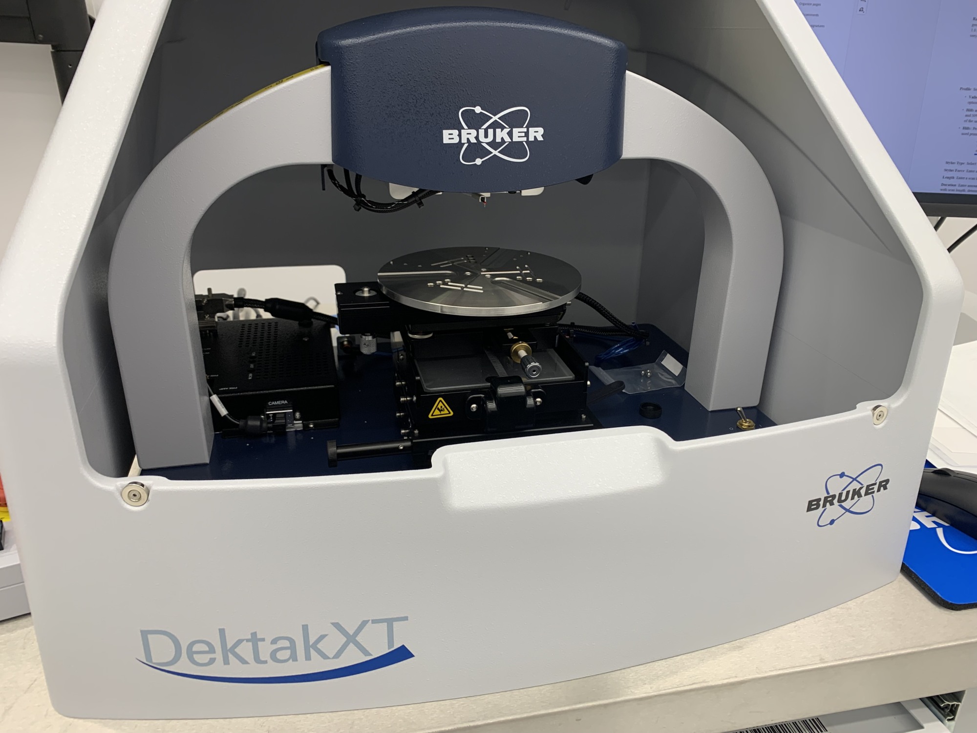
The DektakXT is a unique tool, the result of more than 50 years of research and development, and it represents the state-of-the-art “gold-standard” in stylus profilers. The system comprises an all-in-one stylus sensor that enables simultaneous large vertical range and low-force scanning, and it allows for advanced mapping of film roughness, morphology, stress, thickness (with a step height resolution of less than 10 nm).
Dektak3 Profilometer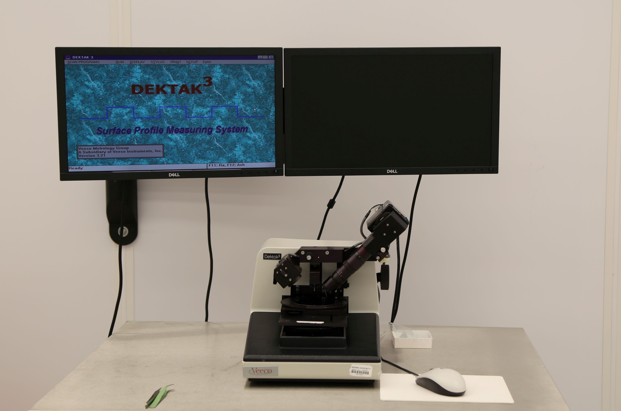
The DekTak3 Profilometer is a computer-controlled surface profile measuring system, which accurately measures step heights from below 50 A to over 50 µm by moving a diamond-tipped stylus over the surface. Equipped with video camera and surface profile analysis software.
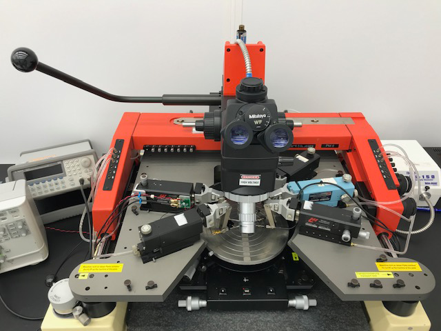
Karl Suss 200mm Precision Manual Analytical Prober
The Karl Suss 200mm Precision Manual Analytical Prober PM8 provides the stability and resolution required for precise probe positioning. Manual submicron semiconductor failure analysis and in-process testing probe station. Submicron precision and stability with a fine-glide chuck stage and 8 in. x 8 in. X-Y movement. As fast as a motorized stage but with the simplicity and resolution of a manual system. Vacuum Chuck: 8 in. dia. Mitutoyo high magnification microscope with two long working distance objectives. Microscope lifts for easier access to the probes and device under test. The station is fitted with six Wentworth micromanipulators having tungsten needle probes with 3 micron tips.
Furnaces
Wet Oxide and Dry Oxide Furnaces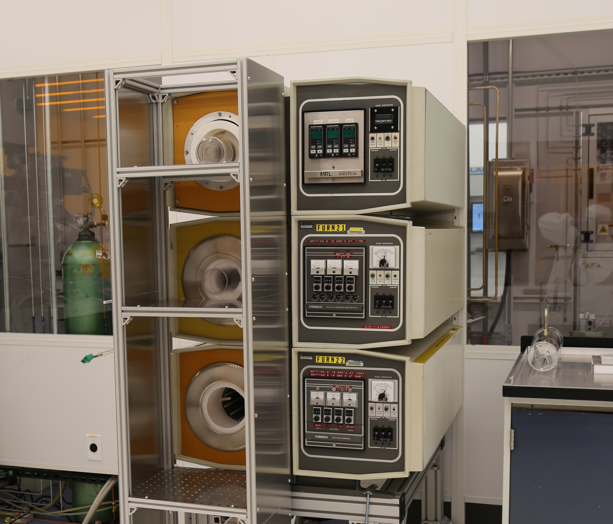
Quartz tube furnaces for thermal oxide growth on silicon by a chemical reaction between the silicon and either dry oxygen or water vapor at atmospheric pressure. The typical temperature range for the oxidation of silicon is 750˚C to 1100˚C. The tubes accommodates multiple 2" wafers.
Wet Chemistry Workbenches
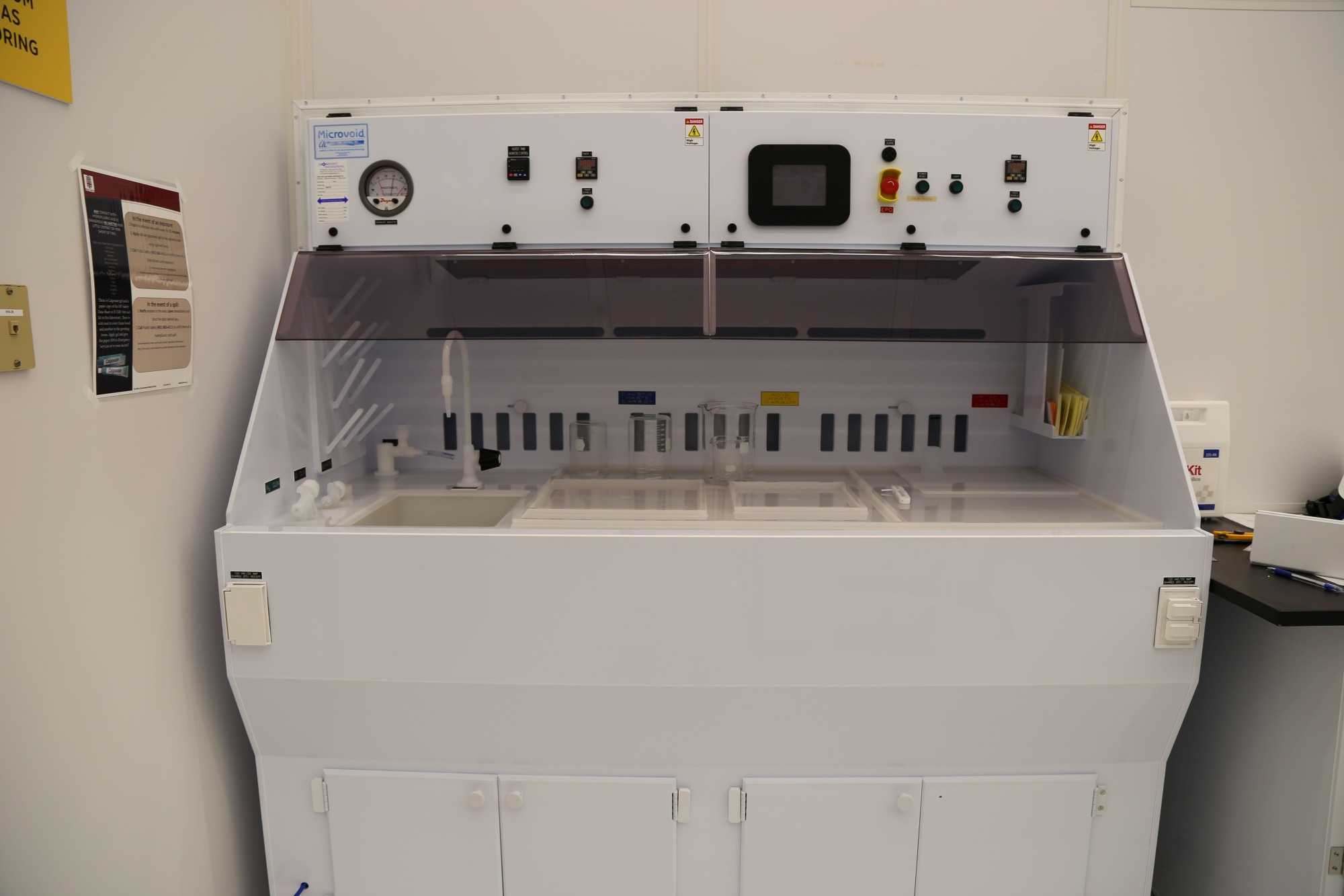
There are five wet chemistry fume hoods, a mix of stainless steel and polymer units. These permit the chemical processing (cleaning, wet etching, electroplating, anodization, etc) employed in the fabrication of semiconductor and microelectronic devices. The stainless steel hoods house spinners for applying photoresist and other polymers for photolithography. Polymer hoods are for cleaning or etching materials with strong acids or bases.